TS-7250-V3 Hardware Manual Test
| WARNING: | This is not the current latest manual for the TS-7250-V3, this is a page for testing new manual layouts. Please return to the TS-7250-V3 manual for the latest up to date manual! |
 | |
| Product Page | |
| Documentation | |
|---|---|
| Schematic | |
| FTP Path | |
| Processor | |
| NXP i.MX6UL | |
| 696 MHz Arm® Cortex®-A7 | |
| i.MX6UL Product Page | |
| CPU Documentation |
Overview
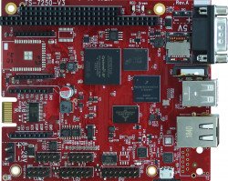
The TS-7250-V3 is a PC/104 form factor SBC with a PC/104 bus, mikroBUS socket, Digi XBee header, soldered down eMMC flash, dual Ethernet, microSD socket, and a Wi-Fi/Bluetooth LE module. This platform also provides a migration path from the TS-7250-V2 and TS-7250 series systems.
Feature Comparison
This platform has multiple hardware variants, please see the TS-7250-V3 product configurations for a comparison of the feature sets by model.
Physical description / connectors / something
IMAGE OF PLATFORM HERE WITH CONNECTORS ANNOTATED IN SOME WAY

Table of different components/features/connectors linked to sections below?
I like the idea of maybe different sections within the table Something like
System I/O
| Feature | Description | Location |
|---|---|---|
| ADC | ADC input | A/D Header / CN8 |
Node Description Location? Jumpers and LEDs jp block | What its for | CNwhatever LED1,2,3 | What they do | CNwhtever Power in | Power input | ... Batt | battery for RTC | ... ? Storage emmc | soldered down | eMMC? sd | SD socket | CNwhatever System IO eth | eth | Twhatever cpu? | cpu | What? USB | usb | CNwhatever CAN | Can interface | COM3 / CN11 ? etc.
Features
Analog-to-Digital Converter (ADC)
This platform offers two groups of analog-to-digital converters (ADCs), one group provided by the CPU, and another group from the Supervisory Microcontroller.
The CPU offers 5 channels of 12-bit ADC inputs. All channels can sample 0-30 V, with channels 1-3 selectively able to sample 0-20 mA current loop input (dynamically enabled by setting the relevant GPIO pin to a logical 1). To minimize noise, the ADC pins use a dedicated analog ground available on the even pins of the header. See the ADC Header section for more details.
The Supervisory Microcontroller offers 5 channels of 12-bit ADC inputs. These are not intended for general purpose and instead are used to read system voltages. These channels monitor the internal 3.3 V rail, VDD_ARM, VDD_SOC, the internal 5 V rail (which can either be generated from the 8-48 V power input rail or directly applied to the 5 V input rail), and then the voltage present on the 8-48 V input.
The ADC inputs are accessible through Linux Industrial I/O (IIO). See the software manual for the software image in use (boy that needs to be worded better) for more information.
| ADC # | IIO Device | IIO Channel | Max Sample Rate[1] | Voltage Range (resolution) | Current Range (resolution) | Current Loop Enable GPIO | Location |
|---|---|---|---|---|---|---|---|
| CPU ADC1 | 2198000.adc | voltage0 | 206 kHz | 0-30 V (~9.7 mV) | 0-20 mA | 20ac000.gpio 7 | ADC Header pin 1 |
| CPU ADC2 | 2198000.adc | voltage1 | 206 kHz | 0-30 V (~9.7 mV) | 0-20 mA | 20ac000.gpio 8 | ADC Header pin 3 |
| CPU ADC6 | 2198000.adc | voltage5 | 206 kHz | 0-30 V (~9.7 mV) | 0-20 mA | 20ac000.gpio 9 | ADC Header pin 5 |
| CPU ADC9 | 2198000.adc | voltage8 | 206 kHz | 0-30 V (~9.7 mV) | -- | -- | ADC Header pin 7 |
| CPU ADC10 | 2198000.adc | voltage9 | 206 kHz | 0-30 V (~9.7 mV) | -- | -- | ADC Header pin 9 |
| WIZ ADC0 | an_3p3v | voltage0 | 700 Hz | -- | -- | -- | Int. 3.3 V rail |
| WIZ ADC1 | tssupervisor-adc | voltage1 | 700 Hz | -- | -- | -- | Int. VDD_ARM_CAP rail |
| WIZ ADC2 | tssupervisor-adc | voltage2 | 700 Hz | -- | -- | -- | Int. VDD_SOC_CAP rail |
| WIZ ADC3 | an_5v | voltage0 | 700 Hz | -- | -- | -- | Int. 5 V rail[2] |
| WIZ ADC4 | an_8v_48v | voltage0 | 700 Hz | -- | -- | -- | 8-48 V input connector |
- ↑ Maximum rate the ADC peripheral can sample at via Linux kernel interface.
- ↑ Either directly from the 5 V input connector, or generated 5 V rail from the 8-48 V input rail.
Battery-Backed Real-Time Clock (RTC)
The TS-7250-V3 RTC is contained as part of the Supervisory Microcontroller. The RTC is driven by a 32,768 Hz oscillator that is ±20 ppm (typ. @ 25°C) and is specified with a first-year aging rate of ±3 ppm. The RTC supports a number of features including:
- Alarm -- An Alarm for use as a wake-up source (to wake the Supervisory Microcontroller from a sleep state, as well as a watchdog timer with a long time frame)
- Battery Detection -- Latched by the RTC at Supervisory Microcontroller power-on and reboot, returns true if measured voltage is > 1.8-2.0 V
- Offset -- Oscillator accuracy offset in parts per billion (ppb)
- An average 8 year runtime on a single CR1632 coin cell -- RTC will operate down to ~1.65 V
While the RTC is contained inside of the Supervisory Microcontroller, it is a separate and independent peripheral that is presented on the same I2C bus.
In Linux, the RTC is supported via our rtc-tssupervisor driver which exposes the Alarm, battery detection, and offset of the crystal accuracy. See the relevant software manual for more information on this (this needs to be worded better).
Bluetooth
The TS-7250-V3 supports Bluetooth 5.0 LE via the WILC3000 Wi-Fi / Bluetooth module.
See the software manual for the software image in use (boy that needs to be worded better) for more information on bringing up and testing the interface.
Both Wi-Fi and Bluetooth can be active at the same time on this platform. Note however, that either the Wi-Fi interface needs to be not brought up if Wi-Fi is unused, or it needs to actively connect to an access point or act as an access point.
Bringing up the Bluetooth Device
# Enable Bluetooth
echo BT_POWER_UP > /dev/wilc_bt ; sleep 1

# Load Bluetooth firmware
echo BT_DOWNLOAD_FW > /dev/wilc_bt ; sleep 1
Once enabled and firmware loaded, the Bluetooth interface is available on the UART device /dev/ttymxc2 at 115200 baud with no flow control.
The module supports other control commands as well:
# Allow the BT chip to enter sleep mode
echo BT_FW_CHIP_ALLOW_SLEEP > /dev/wilc_bt

# Power down the BT radio when not in use
echo BT_POWER_DOWN > /dev/wilc_bt
CAN
The i.MX6UL CPU has two FlexCAN ports which are available on the COM3 Header / CN11.
Both ports conform to CAN 2.0B and ISO 11898 specifications, allowing for communication at speeds up to 1 Mbaud with high noise immunity.
CAN interfaces on the TS-7250-V3 do not provide built-in bus termination resistors. This allows the interfaces to be placed anywhere along the CAN bus. Termination resistors should be added at the ends of the CAN bus where required.
| CAN # | CAN Dev. | CAN_H Loc. | CAN_L Loc. |
|---|---|---|---|
| CPU FLEXCAN1 | can0 | COM3 Header pin 4 | COM3 Header pin 9 |
| CPU FLEXCAN2 | can1 | COM3 Header pin 1 | COM3 Header pin 6 |
See the corresponding software manual for information on interfacing with the CAN hardware (this needs to be reworded and linked better).
CPU
This device uses the i.MX6UL CPU, running at up to 696 MHz, based upon a Cortex-A7 core and targeting low power consumption.
Refer to NXP's documentation for more detailed information on the i.MX6UL.
GPIO
The i.MX6UL GPIO are all exposed in Linux using the gpiod interface.
See the software manual for the software image in use (boy that needs to be worded better) for more information on interfacing with GPIO pins.
For information on the I/O Type and Pull/Keeper of the pins, see the Location information for the relevant pin.
| Line Name[1] | GPIO Chip Label | Line | Location |
|---|---|---|---|
| AN_CH1 [2] | 209c000.gpio | 0 | ADC Pin 1 |
| AN_CH2 [2] | 209c000.gpio | 1 | ADC Pin 3 |
| EN_SD_CARD_3.3V [3] | 209c000.gpio | 4 | Onboard |
| AN_CH3 [2] | 209c000.gpio | 5 | ADC Pin 5 |
| AN_CH4 [2] | 209c000.gpio | 8 | ADC Pin 7 |
| AN_CH5 [2] | 209c000.gpio | 9 | ADC Pin 9 |
| NIMBEL_RESET# | 209c000.gpio | 10 | XBee Header pin 5 |
| SEL_XBEE_USB [4] | 209c000.gpio | 11 | Onboard USB MUX |
| FPGA_RESET [5] | 209c000.gpio | 13 | Onboard |
| EN_RED_LED# [6] | 209c000.gpio | 18 | Onboard LED5 |
| EN_GRN_LED# [6] | 209c000.gpio | 19 | Onboard LED2 |
| EN_XBEE_USB [3] | 209c000.gpio | 21 | Onboard |
| UART4_TXD | 209c000.gpio | 28 | Modem UART |
| UART4_RXD | 209c000.gpio | 29 | Modem UART |
| EN_DIO_FET [7] | 209c000.gpio | 30 | DIO Header pin 4 |
| NIM_PWR_ON | 209c000.gpio | 31 | Onboard |
| EN_USB_5V [8] | 20a4000.gpio | 0 | Onboard |
| NIMBEL_PIN13 | 20a4000.gpio | 2 | XBee Header Pin 13 |
| ISA_RESET | 20a4000.gpio | 7 | PC/104 B2 |
| ISA_IOCHK | 20a4000.gpio | 8 | PC/104 A1 |
| LCD_PIN7 | 20a4000.gpio | 9 | LCD Header pin 7 |
| LCD_PIN8 | 20a4000.gpio | 10 | LCD Header pin 8 |
| LCD_PIN9 | 20a4000.gpio | 11 | LCD Header pin 9 |
| LCD_PIN10 | 20a4000.gpio | 12 | LCD Header pin 10 |
| LCD_PIN11 | 20a4000.gpio | 15 | LCD Header pin 11 |
| LCD_PIN12 | 20a4000.gpio | 16 | LCD Header pin 12 |
| LCD_PIN13 | 20a4000.gpio | 17 | LCD Header pin 13 |
| LCD_PIN14 | 20a4000.gpio | 18 | LCD Header pin 14 |
| LCD_WR# | 20a4000.gpio | 19 | LCD Header pin 6 |
| LCD_EN | 20a4000.gpio | 20 | LCD Header pin 5 |
| LCD_RS | 20a4000.gpio | 21 | LCD Header pin 3 |
| SYS_RESET# [9] | 20a4000.gpio | 22 | Onboard |
| FPGA_FLASH_SELECT [3] | 20a8000.gpio | 0 | Onboard |
| DETECT_94-120 [3] | 20a8000.gpio | 1 | Onboard |
| EN_EMMC_3.3V [3] | 20ac000.gpio | 2 | Onboard eMMC |
| WIFI_RESET# | 20ac000.gpio | 5 | Onboard WIFI |
| EN_WIFI_PWR | 20ac000.gpio | 6 | Onboard WIFI |
| EN_CL_1 | 20ac000.gpio | 7 | ADC Current loop enable |
| EN_CL_2 | 20ac000.gpio | 8 | ADC Current loop enable |
| EN_CL_3 | 20ac000.gpio | 9 | ADC Current loop enable |
| DIO_PIN1 | 50004010.fpga_gpio | 1 | DIO Header pin 1 |
| DIO_PIN3 | 50004010.fpga_gpio | 2 | DIO Header pin 3 |
| DIO_PIN5 | 50004010.fpga_gpio | 3 | DIO Header pin 5 |
| DIO_PIN7 | 50004010.fpga_gpio | 4 | DIO Header pin 7 |
| DIO_PIN8 | 50004010.fpga_gpio | 5 | DIO Header pin 8 |
| DIO_PIN9 | 50004010.fpga_gpio | 6 | DIO Header pin 9 |
| DIO_PIN11 | 50004010.fpga_gpio | 7 | DIO Header pin 11 |
| DIO_PIN13 | 50004010.fpga_gpio | 8 | DIO Header pin 13 |
| DIO_PIN15 | 50004010.fpga_gpio | 9 | DIO Header pin 15 |
| DIO_SPI_MISO [10] | 50004010.fpga_gpio | 10 | SPI MISO |
| DIO_SPI_CS# [11] | 50004010.fpga_gpio | 11 | DIO Header pin 6 |
| DIO_SPI_CLK [11] | 50004010.fpga_gpio | 14 | DIO Header pin 14 |
| DIO_SPI_MOSI [11] | 50004010.fpga_gpio | 15 | DIO Header pin 12 |
| ISA_AEN [12] | 50004040.fpga_gpio | 0 | PC/104 Header pin A11 |
| ISA_BALE | 50004040.fpga_gpio | 1 | PC/104 Header pin B28 |
| ISA_TC | 50004040.fpga_gpio | 2 | PC/104 Header pin B27 |
| ISA_ENDX | 50004040.fpga_gpio | 3 | PC/104 Header pin B08 |
| EN_NIMBEL_3V3 | 50004040.fpga_gpio | 4 | Skywire VIN voltage |
| ISA_IORDY | 50004040.fpga_gpio | 5 | PC/104 Header pin A10 |
| ISA_REFRESH | 50004040.fpga_gpio | 6 | PC/104 Header pin B19 |
| ISA_DRQ1 | 50004040.fpga_gpio | 7 | PC/104 Header pin B18 |
| ISA_DACK1 | 50004040.fpga_gpio | 8 | PC/104 Header pin B17 |
| ISA_DRQ2 | 50004040.fpga_gpio | 9 | PC/104 Header pin B06 |
| ISA_DACK2 | 50004040.fpga_gpio | 10 | PC/104 Header pin B26 |
| EN_NIMBEL_4V | 50004040.fpga_gpio | 11 | Skywire VIN voltage |
| ISA_DRQ3 | 50004040.fpga_gpio | 12 | PC/104 Header pin B16 |
| ISA_DACK3 | 50004040.fpga_gpio | 13 | PC/104 Header pin B15 |
| MIKRO_RESET# | 50004054.fpga_gpio | 0 | mikroBUS Header pin 2 |
| MIKRO_AN | 50004054.fpga_gpio | 1 | mikroBUS Header pin 1 |
| MIKRO_INT | 50004054.fpga_gpio | 2 | mikroBUS Header pin 15 |
| MIKRO_180 [13] | 50004054.fpga_gpio | 3 | Onboard |
| MIKRO_PWM [14] | 50004054.fpga_gpio | 4 | mikroBUS Header pin 16 |
| MIKRO_SPI_CS# [15] | 50004054.fpga_gpio | 5 | mikroBUS Header pin 3 |
| MIKRO_SPI_CLK [15] | 50004054.fpga_gpio | 6 | mikroBUS Header pin 4 |
| MIKRO_SPI_MISO [15] | 50004054.fpga_gpio | 7 | mikroBUS Header pin 5 |
| MIKRO_SPI_MOSI [15] | 50004054.fpga_gpio | 8 | mikroBUS Header pin 6 |
| MIKRO_TXD [16] | 50004054.fpga_gpio | 9 | mikroBUS Header pin 13 |
| MIKRO_RXD [16] | 50004054.fpga_gpio | 10 | mikroBUS Header pin 14 |
| MIKRO_I2C_DAT [17] | 50004054.fpga_gpio | 11 | mikroBUS Header pin 11 |
| MIKRO_I2C_CLK [17] | 50004054.fpga_gpio | 12 | mikroBUS Header pin 12 |
| ISA_DAT00 [12] | 5000405c.fpga_gpio | 0 | PC/104 Header pin A9 |
| ISA_DAT01 [12] | 5000405c.fpga_gpio | 1 | PC/104 Header pin A8 |
| ISA_DAT02 [12] | 5000405c.fpga_gpio | 2 | PC/104 Header pin A7 |
| ISA_DAT03 [12] | 5000405c.fpga_gpio | 3 | PC/104 Header pin A6 |
| ISA_DAT04 [12] | 5000405c.fpga_gpio | 4 | PC/104 Header pin A5 |
| ISA_DAT05 [12] | 5000405c.fpga_gpio | 5 | PC/104 Header pin A4 |
| ISA_DAT06 [12] | 5000405c.fpga_gpio | 6 | PC/104 Header pin A3 |
| ISA_DAT07 [12] | 5000405c.fpga_gpio | 7 | PC/104 Header pin A2 |
| ISA_DAT08 [12] | 5000405c.fpga_gpio | 8 | PC/104 Header pin C11 |
| ISA_DAT_09 [12] | 5000405c.fpga_gpio | 9 | PC/104 Header pin C12 |
| ISA_DAT10 [12] | 5000405c.fpga_gpio | 10 | PC/104 Header pin C13 |
| ISA_DAT11 [12] | 5000405c.fpga_gpio | 11 | PC/104 Header pin C14 |
| ISA_DAT12 [12] | 5000405c.fpga_gpio | 12 | PC/104 Header pin C15 |
| ISA_DAT13 [12] | 5000405c.fpga_gpio | 13 | PC/104 Header pin C16 |
| ISA_DAT14 [12] | 5000405c.fpga_gpio | 14 | PC/104 Header pin C17 |
| ISA_DAT15 [12] | 5000405c.fpga_gpio | 15 | PC/104 Header pin C18 |
| ISA_ADD_00 [12] | 50004064.fpga_gpio | 0 | PC/104 Header pin A31 |
| ISA_ADD_01 [12] | 50004064.fpga_gpio | 1 | PC/104 Header pin A30 |
| ISA_ADD_02 [12] | 50004064.fpga_gpio | 2 | PC/104 Header pin A29 |
| ISA_ADD_03 [12] | 50004064.fpga_gpio | 3 | PC/104 Header pin A28 |
| ISA_ADD_04 [12] | 50004064.fpga_gpio | 4 | PC/104 Header pin A27 |
| ISA_ADD_05 [12] | 50004064.fpga_gpio | 5 | PC/104 Header pin A26 |
| ISA_ADD_06 [12] | 50004064.fpga_gpio | 6 | PC/104 Header pin A25 |
| ISA_ADD_07 [12] | 50004064.fpga_gpio | 7 | PC104 Header pin A24 |
| ISA_ADD_08 [12] | 50004064.fpga_gpio | 8 | PC104 Header pin A23 |
| ISA_ADD_09 [12] | 50004064.fpga_gpio | 9 | PC104 Header pin A22 |
| ISA_ADD_10 [12] | 50004064.fpga_gpio | 10 | PC104 Header pin A21 |
| ISA_ADD_11 [12] | 50004064.fpga_gpio | 11 | PC104 Header pin A20 |
| ISA_ADD_12 [12] | 50004064.fpga_gpio | 12 | PC104 Header pin A19 |
| ISA_ADD_13 [12] | 50004064.fpga_gpio | 13 | PC104 Header pin A18 |
| ISA_ADD_14 [12] | 50004064.fpga_gpio | 14 | PC104 Header pin A17 |
| ISA_ADD_15 [12] | 50004064.fpga_gpio | 15 | PC104 Header pin A16 |
| ISA_ADD_16 [12] | 5000406c.fpga_gpio | 0 | PC104 Header pin A15 |
| ISA_ADD_17 [12] | 5000406c.fpga_gpio | 1 | PC104 Header pin A14 |
| ISA_ADD_18 [12] | 5000406c.fpga_gpio | 2 | PC/104 Header pin A13 |
| ISA_ADD_19 [12] | 5000406c.fpga_gpio | 3 | PC/104 Header pin A12 |
| ISA_IOR# [12] | 5000406c.fpga_gpio | 4 | PC/104 Header pin B14 |
| ISA_IOW# [12] | 5000406c.fpga_gpio | 5 | PC/104 Header pin B13 |
| ISA_MEMR# [12] | 5000406c.fpga_gpio | 6 | PC/104 Header pin B12 |
| ISA_MEMW# [12] | 5000406c.fpga_gpio | 7 | PC104 Header pin B11 |
| ISA_CN_D01 | 5000406c.fpga_gpio | 8 | PC104 Header pin D01 |
| ISA_CN_D02 | 5000406c.fpga_gpio | 8 | PC104 Header pin D02 |
| ISA_CN_D03 | 2-0020 | 0 | PC104 Header pin D03 |
| ISA_CN_D04 | 2-0020 | 1 | PC104 Header pin D04 |
| ISA_CN_D05 | 2-0020 | 2 | PC104 Header pin D05 |
| ISA_CN_D06 | 2-0020 | 3 | PC104 Header pin D06 |
| ISA_CN_D07 | 2-0020 | 4 | PC104 Header pin D07 |
| ISA_CN_D08 | 2-0020 | 5 | PC104 Header pin D08 |
| ISA_CN_D09 | 2-0020 | 6 | PC104 Header pin D09 |
| ISA_CN_D10 | 2-0020 | 7 | PC104 Header pin D10 |
| ISA_CN_D11 | 2-0020 | 8 | PC104 Header pin D11 |
| ISA_CN_D12 | 2-0020 | 9 | PC104 Header pin D12 |
| ISA_CN_D13 | 2-0020 | 10 | PC104 Header pin D13 |
| ISA_CN_D14 | 2-0020 | 11 | PC104 Header pin D14 |
| ISA_CN_D15 | 2-0020 | 12 | PC104 Header pin D15 |
- ↑ The line name exported by the Linux kernel matches the schematic net name for easy cross reference.
- ↑ 2.0 2.1 2.2 2.3 2.4 Do not enable the current-loop measurement mode if using this pin as a GPIO. It may cause damage to the circuit if not properly current limited.
- ↑ 3.0 3.1 3.2 3.3 3.4 This is controlled automatically on startup to give the SD card a clean reset, but otherwise this should not be toggled manually.
- ↑ default is input with pulldown (0). If driven high, this MUXes the bottom port of the dual high USB port to the XBee header. If low or input, no USB is present on this header. This USB is needed for cell modules, but interferes with older serial modules where these USB pins are reserved. See your XBee/Skywire device's datasheet to verify if USB is needed.
- ↑ This is handled automatically on startup
- ↑ 6.0 6.1 See the LEDs section for interacting with these LEDs rather than toggling the GPIO directly.
- ↑ The I/O Specifications and pull/keeper for this pin are at the DIO header and not the GPIO that controls the enable.
- ↑ High by default. This allows power cycling USB peripherals in the field.
- ↑ Ethernet PHY and USB hub reset. This is automatically controlled during startup and should not be toggled.
- ↑ This pin is input only.
- ↑ 11.0 11.1 11.2 This pin cannot be controlled as a GPIO until Syscon 0x08 bit 10 is set
- ↑ 12.00 12.01 12.02 12.03 12.04 12.05 12.06 12.07 12.08 12.09 12.10 12.11 12.12 12.13 12.14 12.15 12.16 12.17 12.18 12.19 12.20 12.21 12.22 12.23 12.24 12.25 12.26 12.27 12.28 12.29 12.30 12.31 12.32 12.33 12.34 12.35 12.36 12.37 12.38 12.39 12.40 This pin cannot be controlled as a GPIO until Syscon 0x08 bit 8 is set
- ↑ This is used to detect if the Mikrobus socket is reversed.
- ↑ This pin cannot be controlled as a GPIO until Syscon 0x08 bit 6 is set
- ↑ 15.0 15.1 15.2 15.3 This pin cannot be controlled as a GPIO until Syscon 0x08 bit 4 is set
- ↑ 16.0 16.1 This pin cannot be controlled as a GPIO until Syscon 0x08 bit 7 is set
- ↑ 17.0 17.1 This pin cannot be controlled as a GPIO until Syscon 0x08 bit 5 is set
eMMC
This platform includes a soldered down eMMC flash device for on-board non-volatile storage. Our standard platform configurations use a 4 GB eMMC device, but up to 64 GB are available for customized builds. The eMMC device includes additional boot partitions that are used by U-Boot and are not affected by the disk's partition table.
The soldered down eMMC on the TS-7250-V3 averages speeds of 5500 KiB/s for both read and write to files within the filesystem.
See the software manual for the software image in use (boy that needs to be worded better) for more information.
In Linux, the eMMC device appears as /dev/mmcblk0 and our stock images use the following disk layout:
| Device | Contents |
|---|---|
| /dev/mmcblk0 | eMMC block device |
| /dev/mmcblk0boot0 | U-Boot |
| /dev/mmcblk0boot1 | Unused |
| /dev/mmcblk0p1 | Full Debian Linux partition |
SHOULD THIS MANUAL TALK ABOUT ENH MODES? CREATE ANOTHER MANUAL FOR IT?
Ethernet Ports
The i.MX6UL CPU contains two 10/100 Mbit Ethernet controllers with support built into the Linux kernel. These are located at the two Ethernet connector jacks on the platform.
These interfaces can appear to the user as eth0 and eth1; or as end0 and end1 depending on the kernel version and Linux's dynamic device management configuration.
The i.MX6UL CPU Ethernet ports support IEEE 1588 Precision Time Protocol (PTP), both Version 1 and 2 (PTPv1 & PTPv2). This allows synchronizing the system clock to within ±1 us across multiple devices on the same network.
See the software manual for the software image in use (boy that needs to be worded better) for more information on utilizing the interfaces as well as setting up PTP.
Ferroelectric RAM (FRAM)
| Note: | FRAM is not present on the TS-7250-V3-SMN1I or TS-7250-V3-SMN2I configurations. |
This device supports an optional 2 KiB of non-volatile Ferroelectric RAM (FRAM) connected to the CPU via SPI. FRAM is non-volatile, incredibly fast to write, and is specified with 1 trillion read/write cycles per each byte with a 200 year data retention. Reads of data from FRAM is a destructive process -- the FRAM's internal controller handles data write-back after a read. Care should be taken to prevent sudden power-off events during both reads and writes of FRAM.
The FRAM is connected to the TS-7250-V3 on FPGA SPI0, chip-select 1.
Should this list IIO device and channel?
See the software manual for the software image in use (boy that needs to be worded better) for information on interacting with the device.
I2C
The i.MX6UL supports I2C at 100 kHz, or using fast mode for 400 kHz operation. The TS-7250-V3 uses two CPU I2C busses for onboard device, and an FPGA I2C controller for the mikroBUS I2C interface.
See the software manual for the software image in use (boy that needs to be worded better) for more information.
The list of I2C busses below are by their bus number as well as the device number the Linux kernel enumerates them as.
| I2C # | I2C Dev. | Address | Description |
|---|---|---|---|
| CPU I2C1 | i2c-0 | 0x1e | Magnetometer |
| 0x54 | Supervisory Microcontroller | ||
| 0x68 | RTC | ||
| 0x6a | IMU | ||
| CPU I2C3 | i2c-2 | 0x20 | NXP pca9555 GPIO expander (Chip 2-0020) |
| 0x64 | ATSHA204 LINK TO MORE INFO [1] | ||
| FPGA I2C0 | i2c-4 | N/A | mikroBUS I2C interface |
- ↑ Not populated by default
TODO: Add mikroBUS I2C notes
Inertial Measurement Unit (IMU)
| Note: | The IMU is not present on the TS-7250-V3-SMN1I or TS-7250-V3-SMN2I configurations. |
The TS-7250-V3 includes a soldered down 9 degrees of freedom Internal Measurement Unit (IMU) using a two-component solution with a ST ISM330 for the accelerometer and gyroscope, and a ST IIS2MDCTR magnetometer.
The ST ISM330 offers a selectable full-scale acceleration range of ±2/±4/±8/±16 g, and an angular rate range of ±125/±250/±500/±1000/±2000 dps. The ST IIS2MDCTR offers a magnetic field dynamic range of ±50 gauss.
Both devices are connected to the platform via the CPU I2C1 bus and are connected to Linux's Industrial I/O (IIO) subsystem. The IIO subsystem provides both userspace tools via iio-tools and libiio for interface libraries to interact with these devices.
See the software manual for the software image in use (boy that needs to be worded better) for information on interacting with the IMU.
Interrupts
| Note: | This section is incomplete at this time. |
LEDs
This platform has two on-board LEDs near the 5 V power input and PC/104 header. U-Boot uses these to indicate stages of boot, and the Linux kernel turns on the green LED and the red LED off by default. After that point, the LEDs are able to be directly controlled from userspace; either manually or using a number of system triggers.
Depending on the kernel version being booted, the LEDs may present themselves with slightly different names. On this platform, the pattern may be either of the following:
<color>-led- e.g.
green-led
- --OR--
<color>:<purpose>- e.g.
green:power
See the relevant software manual for more information on controlling the LEDs.
MicroSD Interface
The i.MX6UL SDHCI driver supports microSD cards up to and including microSDXC standards, supporting up to 2 TB of storage.
TALK ABOUT SPEEDS
Appears at /dev/mmcblk1
We have performed compatibility testing on the Sandisk MicroSD cards we provide. We do not suggest switching brands/models without your own qualification testing. While SD cards specifications are standardized, in practice cards behave very differently. We do not recommend ATP or Transcend MicroSD cards due to known compatibility issues. IS THIS STILL AN ISSUE?!
MicroSD cards should not have power removed during a write or they will have disk corruption. Keep the filesystem mounted read only if this is a possibility. It is not always possible for fsck to recover from the types of failures that will be seen with SD power loss. Consider using the eMMC for storage instead which is far more resilient to power loss.
Supervisory Microcontroller
| Note: | The features outlined below are only supported in Linux kernel 5.10 and later, and on PCB revision C (early 2023) and later. |
The TS-7250-V3 includes a preprogrammed microcontroller designed to:
- Manage the platforms's power state (including a low-power 25 mW power-off state)
- Provide a real-time clock (RTC) (including alarm wake functionality)
- Provide a temperature sensor
- Provide analog-to-digital converters (ADCs) for measuring onboard voltage rails
- Provide the USB console functionality for the platform
USB Console Configuration
By default, the TS-7250-V3 serial console is run through the DB-9 Connector using RS-232 signaling. However, if a micro USB cable is connected between the TS-7250-V3's micro USB socket and a USB host, the Supervisory Microcontroller will enumerate a USB serial device on the USB host side; routing the serial console to the USB interface and away from the serial port present on the DB-9 connector.
Anytime the CPU UART1 serial console is routed to USB, FPGA UART0 is routed to the DB-9 port for application use.
The Supervisory Microcontroller can be configured to always route the console through the micro USB port instead of auto-selection based on USB connection to a host.
In Linux on the TS-7250-V3, this setting is exposed via sysfs:
root@tsimx6ul:~# cat /sys/bus/i2c/devices/0-0010/console_cfg
[auto] always-usb
root@tsimx6ul:~# echo "always-usb" > /sys/bus/i2c/devices/0-0010/console_cfg
root@tsimx6ul:~# cat /sys/bus/i2c/devices/0-0010/console_cfg
auto [always-usb]
Setting always-usb will cause CPU UART1 serial console to always be routed through the micro USB serial interface (regardless of it is connected to a USB host), leaving FPGA UART0 always routed to the DB-9 connector for application use.
Power Control and Reset
Under compatible operating systems, the Supervisory Microcontroller has a reset controller driver available in order to manage reboot and power-off states. In these environments, the Supervisory Microcontroller can reboot, halt, and power off the platform to the fullest extent that the operating system provides. The latter of which, power-off, signals the microcontroller to remove power from the rest of the platform once the kernel has fully halted.
Low-Power Mode
If the operating system initiates a power-off sequence, the Supervisory Microcontroller will remove power from the rest of the platform when approperiate and then enters a low power state. This leaves only the Supervisory Microcontroller powered on. In this state the whole platform will only consume about 25 mW.
The Supervisory Microcontroller will remain in a lower power state until one of the following events occurs. At which time it will wake up and enable power to the rest of the platform to let it begin a normal boot process.
- CN8 ADC Header pin 9 input voltage rose above 3 V
- 5 VDC rail[1] goes below 4.7 VDC, and then back above 4.7 VDC.
- Real-time clock (RTC) Alarm expired
- Micro USB serial console was connected to a USB host
Wake/Reset Reason
The Supervisory Microcontroller tracks the most recent event which caused the system to reboot or turn on. Under compatible operating systems, this is exposed as part of the reset controller driver.
In Linux on the TS-7250-V3, this information is exposed via sysfs:
root@tsimx6ul:~# cat /sys/bus/platform/devices/tssupervisor-reset/reboot_reason
POR
| reboot_reason text | Description |
|---|---|
| POR | Initial power-on reset after both micro USB serial console and VIN[2] were removed |
| Brownout | 5 VDC rail[1] dropped below 4.7 V but Supervisory Microcontroller power input remained valid |
| CPU WDT | Watchdog timer (WDT) expired and caused a hardware reboot |
| Software Reboot | The operating system initiated a reboot |
| RTC Alarm Reboot | Real-time clock (RTC) alarm expired and was configured to cause a hardware reboot |
| Wake from PWR Cycle | The operating system initiated a power-off, after which VIN[2] was cycled off and back on |
| Wake from WAKE_EN | The operating system initiated a power-off, after which the voltage input on ADC Header pin 9 rose from below 1 V to above 3 V |
| Wake from USB VBUS | The operating system initiated a power-off, after which a micro USB serial console cable was connected to USB host |
| Wake from RTC Alarm | The operating system initiated a power-off, after which the real-time clock (RTC) alarm expired |
SPI
DISCUSS WILC SPI? I2C TALKS ABOUT ON-BOARD BUSSES THAT ARE OTHERWISE UNUSABLE? The TS-7250-V3 provides two SPI busses.
SPI devices are recommended to be connected to a kernel driver, though it is possible to arbitrarily interface to SPI devices using the spidev kernel interface. See the software manual for the software image in use (boy that needs to be worded better) for more information.
The TS-7250-V3 FPGA includes the 2 opencore SPI controllers. Under Linux these are spi4 and spi5.
SHOULD THIS MENTION DEVICE NODE NAMES/NUMBER/FIRST BUS/SECOND BUS/ETC?
| SPI # | SPI Dev. | Device |
|---|---|---|
| CPU SPI3 | spidev2.0 | On-board Wi-Fi module |
| FPGA SPI0 | spidev4.0 | DIO Header SPI bus |
| spidev4.1 | Ferroelectric RAM (FRAM) | |
| spidev4.2 | FPGA Flash (/dev/mtdblock0) [1] | |
| FPGA SPI1 | spidev5.0 | mikroBUS SPI |
Temperature Sensor
The TS-7250-V3 contains two temperature sensors, one internal to the CPU and one internal to the Supervisory Microcontroller to monitor die temperatures of both.
The Supervisory Microcontroller temperature sensor can be used to read the ambient temperature as the Supervisory Microcontroller junction temperature has a constant relationship with the IC case temperature.
In Linux, the CPU temperature sensor has a critical junction temperature limit configured. If met, the kernel will do an emergency shutdown of the system to prevent damage.
See the relevant software manual for information on reading the sensor data.
| Sensor # | Sensor Name | Sensor Channel | Scale |
|---|---|---|---|
| CPU TEMP0 | imx_thermal_zone | temp1 | millidegrees Celsius |
| WIZ TEMP0 | supervisor_temp | temp1 | millidegrees Celsius |
UARTs
The TS-7250-V3 includes UARTs on the CPU, as well as 16550A compatible registers on the FPGA interface.
See the software manual for the software image in use (boy that needs to be worded better) for more information.
THESE SHOULD INCLUDE MORE INFORMATION ON WHICH PHYSICAL INTERFACE THEY ARE. OTHER SECTIONS, LIKE GPIO, JUST KIND OF CALL OUT THE NET NAME AND LINK HERE BUT THERE IS NO LINK BETWEEN SOFTWARE ORDERING AND HARDWARE NAME.
| UART # | UART Dev. | Type | TX / + Loc. | RX / - Loc. | CTS | RTS | DCD | DTR | TXEN |
|---|---|---|---|---|---|---|---|---|---|
| CPU UART1 | ttymxc0 | USB Console | P2 MicroUSB | P2 MicroUSB | N/A | N/A | N/A | N/A | N/A |
| CPU UART3 | ttymxc2 | Bluetooth | Onboard | Onboard | N/A | N/A | N/A | N/A | N/A |
| CPU UART4 | ttymxc3 | 3.3V TTL | XBee pin 3 | XBee pin 2 | XBee pin 12 | N/A | N/A | N/A | N/A |
| FPGA UART0 | ttyS8 | RS-232 | DB9 pin 3 | DB9 pin 2 | DB9 pin 8 | DB9 pin 7 | DB9 pin 1 | DB9 pin 4 | N/A |
| FPGA UART1 | ttyS9 | RS-232 | COM2 pin 3 | COM2 pin 2 | COM2 pin 8 | COM2 pin 7 | N/A | N/A | N/A |
| FPGA UART2 | ttyS10 | RS-232 | COM3 pin 3 | COM3 pin 2 | COM3 pin 8 | COM3 pin 7 | N/A | N/A | N/A |
| FPGA UART3 | ttyS11 | RS-485 | COM2 pin 1 | COM2 pin 6 | N/A | N/A | N/A | N/A | N/A |
| FPGA UART4 | ttyS12 | RS-485 | COM2 pin 4 | COM2 pin 9 | N/A | N/A | N/A | N/A | N/A |
| FPGA UART5 | ttyS13 | TTL | mikroBUS pin 13 | mikroBUS pin 14 | N/A | N/A | N/A | N/A | N/A |
| FPGA UART6 | ttyS14 [1] | TTL | DIO pin 5 | DIO pin 7 | N/A | N/A | N/A | N/A | DIO pin 13 |
| FPGA UART7 | ttyS15 [1] | TTL | DIO pin 9 | DIO pin 11 | N/A | N/A | N/A | N/A | DIO pin 15 |
| FPGA UART8 | ttyS16 |
- ↑ 1.0 1.1 Not enabled until setting #FPGA Syscon 0x08 bit 9 to 1
The DIO header uarts, ttyS14 and ttyS15 are not enabled until a mux register is set.
# Change DIO header to use UARTs instead of GPIO
tshwctl --address 0x08 --poke32 0x6000
RS-485
RS-485 is implemented via a UART interface inside of the FPGA. This device handles automatic TXEN assertion and de-assertion for half-duplex RS-485 communication without any required settings or API calls. See the UARTs section for the location of the RS-485 port.
RS-422
While both ttyS11 and ttyS12 support RS-485 half duplex these uarts can also be used as a single full duplex RS-422. Either of these UARTs are electrically compatible with RS-485/RS-422 and support TX or RX. To implement RS-422 in software open either UART and use it for transmit, and open the other UART and only use it for receive.
USB
The TS-7250-V3 offers two USB 2.0 host ports. Power to the host ports can be controlled via GPIO EXPLAIN WHICH.
See the software manual for the software image in use (boy that needs to be worded better) for more information. NOTE THAT THERE MAY BE KERNEL DIFFERENCES! ORIGINAL MANUAL TALKS ABOUT STILL USING THE BRIGHTNESS FILE, WHEREAS IN 5.10/6.6 ITS A GPIO PROPERLY.
The USB A host port stack can provide 1 A total power output shared between the two ports.
Watchdog Timer (WDT)
The TS-7250-V3 implements a watchdog timer (WDT) inside the CPU. The WDT is designed to issue a hardware reset to the CPU if the timeout is exceeded. The timeout of the WDT is configurable at runtime, and feeding the WDT restarts the current counter of the timeout.
See the software manual for the image in use (word this better) for more information.
WiFi
This board uses an ATWILC3000-MR110CA IEEE 802.11 b/g/n Link Controller Module With Integrated Bluetooth® 4.0. Linux provides support for this module using the wilc3000 driver.
Summary features:
- IEEE 802.11 b/g/n RF/PHY/MAC SOC
- IEEE 802.11 b/g/n (1x1) for up to 72 Mbps PHY rate
- Single spatial stream in 2.4GHz ISM band
- Integrated PA and T/R Switch Integrated Chip Antenna
- Superior Sensitivity and Range via advanced PHY signal processing
- Advanced Equalization and Channel Estimation
- Advanced Carrier and Timing Synchronization
- Wi-Fi Direct and Soft-AP support
- Supports IEEE 802.11 WEP, WPA, and WPA2 Security
- Supports China WAPI security
- Operating temperature range of -40°C to +85°C
External Interfaces
ADC Header
The ADC header is a 0.1" pitch 2x5 header supporting voltage and current measurement from external sources on the TS-7250-V3.
NOTE! ADCs should also list their input impedances! I think this should be a part of the IO spec, but, will figure that out another day.
| Signals | Pin Layout | ||||||||||||||||||||||||||||||||||||||||||||
|---|---|---|---|---|---|---|---|---|---|---|---|---|---|---|---|---|---|---|---|---|---|---|---|---|---|---|---|---|---|---|---|---|---|---|---|---|---|---|---|---|---|---|---|---|---|
|
|

Battery Connector
The Battery-Backed Real-Time Clock (RTC) uses a removable CR1632 coin cell in a vertical mount holder. The cell is inserted from the top of the connector, with the positive lead oriented as in the photo below. Once inserted, metal tabs retain the cell. The cell can be removed by pushing the tabs to the side and pushing the cell up from the bottom of the connector.

COM2 Header
The COM2 header is a 0.1" pitch 2x5 header supporting RS-485, RS-422 (by using the two separate RS-485 ports simultaneously for full-duplex communications), and RS-232.
| Signals | Pin Layout | ||||||||||||||||||||||||||||||||||||||||||||
|---|---|---|---|---|---|---|---|---|---|---|---|---|---|---|---|---|---|---|---|---|---|---|---|---|---|---|---|---|---|---|---|---|---|---|---|---|---|---|---|---|---|---|---|---|---|
|
|

COM3 Header
The COM3 header is a 0.1" pitch 2x5 header supporting CAN and RS-232.
| Signals | Pin Layout | ||||||||||||||||||||||||||||||||||||||||||||
|---|---|---|---|---|---|---|---|---|---|---|---|---|---|---|---|---|---|---|---|---|---|---|---|---|---|---|---|---|---|---|---|---|---|---|---|---|---|---|---|---|---|---|---|---|---|
|
|

DB9 Connector
| Note: | What is routed here depends on the microcontroller console state! Need to update the documentation here to clarify this |
The DB9 (DE-9) connector provides an RS-232 port with full handshakes.
| Signals | Pin Layout | ||||||||||||||||||||||||||||||||||||||||
|---|---|---|---|---|---|---|---|---|---|---|---|---|---|---|---|---|---|---|---|---|---|---|---|---|---|---|---|---|---|---|---|---|---|---|---|---|---|---|---|---|---|
|
|

DIO Header
The DIO header is a 0.1" pitch 2x8 header including SPI, UART, and GPIO. All pins on this header are 5 V tolerant except SPI output pins. It supports our KPAD (talk about this more) somehow.
| Signals | Pin Layout | |||||||||||||||||||||||||||||||||||||||||||||||||||||||||||||||||||||||||||||||||||||
|---|---|---|---|---|---|---|---|---|---|---|---|---|---|---|---|---|---|---|---|---|---|---|---|---|---|---|---|---|---|---|---|---|---|---|---|---|---|---|---|---|---|---|---|---|---|---|---|---|---|---|---|---|---|---|---|---|---|---|---|---|---|---|---|---|---|---|---|---|---|---|---|---|---|---|---|---|---|---|---|---|---|---|---|---|---|---|
|
|


TODO: Make some reference to the KPAD interface. This can be from the original userspace source example, or, there is also a way to connect this to a driver. Should document that as well.
Ethernet connectors
The TS-7250-V3 supports two independent 10/100 Ethernet ports. See the Configuring the Network section of the manual for more information on configuration.

LCD Header
The LCD header is a 0.1" pitch 2x7 header including GPIO. This is designed around compatibility with the HD44780 LCD controller which includes our LCD-LED. The LCD Data pins (7-14) are 5 V tolerant. These will output up to 3.3 V, and the remaining control I/O and PWM are 3.3 V tolerant.
TODO: Talk about LCD interfacing? It will be very linux specific and should probably be in the debian manual
TODO: How to better talk about PWM? Maybe link to FPGA section (has been removed in this manual for testing/clarity)
Pin 4, the LCD_BIAS pin, is used to set the contrast on the LCD.
tshwctl --address 0x1c --poke16 0x0 # Writes minimum
tshwctl --address 0x1c --poke16 0xf # Writes maximum
| Signals | Pin Layout | ||||||||||||||||||||||||||||||||||||||||||||||||||||||||||||
|---|---|---|---|---|---|---|---|---|---|---|---|---|---|---|---|---|---|---|---|---|---|---|---|---|---|---|---|---|---|---|---|---|---|---|---|---|---|---|---|---|---|---|---|---|---|---|---|---|---|---|---|---|---|---|---|---|---|---|---|---|---|
|
|

- ↑ If a resistance value is specified, this means a physical resistor is in-circuit; otherwise an internal pull resistor is enabled for that line.
- ↑ PWM duty cycle controlled by FPGA Syscon reg 0x1C. This may need to be tuned depending on the environment or altitude where the display is used.
mikroBUS Header
The mikroBUS header is a 0.1" pitch 2x8 header which supports the MIKROE Click board™ ecosystem. This header features 3.3 V, 5 V, SPI, GPIO, ADC, I2C, UART, and PWM.
More information on Click Boards and the mikroBUS socket/standards can be found here.
| Signals | Pin Layout | |||||||||||||||||||||||||||||||||||||||||||||||||||||||||||||||||||||||||||||||||||||
|---|---|---|---|---|---|---|---|---|---|---|---|---|---|---|---|---|---|---|---|---|---|---|---|---|---|---|---|---|---|---|---|---|---|---|---|---|---|---|---|---|---|---|---|---|---|---|---|---|---|---|---|---|---|---|---|---|---|---|---|---|---|---|---|---|---|---|---|---|---|---|---|---|---|---|---|---|---|---|---|---|---|---|---|---|---|---|
|
|

- ↑ The I/O type applies whether the pin is used as a GPIO or assigned to a peripheral.
- ↑ If a resistance value is specified, this means a physical resistor is in-circuit; otherwise an internal pull resistor is enabled for that line.
- ↑ This pin can be used as an ADC or a GPIO; the GPIO direction should be set as input (which is the default out of reset) to read the ADC signal properly
MicroSD Connector
The MicroSD socket is located near the DB9 on top of the board. See the #MicroSD Interface section for more details on the CPU controller.

MicroUSB Connector
The TS-7250-V3 features an onboard supervisory microcontroller that converts the onboard 3.3V TTL console UART (ttymxc0) into a CP2103 USB serial device.

PC/104 Header
The PC/104 connector consists of four rows of pins labelled A-D. This header implements a PC/104 bus, with most pins also able to be used as GPIO.

| Pin | Default Function | Alternate Function | I/O Type | Pull/Keeper | Pin | Default Function | Alternate Function | I/O Type | Pull/Keeper |
|---|---|---|---|---|---|---|---|---|---|
| D00 | GND | -- | -- | -- | C00 | GND | -- | -- | -- |
| D01 | GPIO: ISA_CN_D01 | None | LVTTL33_FPGA | 1.5 kΩ Pullup | C01 | Pulled to 3.3 V | -- | -- | 10 kΩ Pullup |
| D02 | GPIO: ISA_CN_D02 | None | LVTTL33_FPGA | 1.5 kΩ Pullup | C02 | NC | -- | -- | -- |
| D03 | GPIO: ISA_CN_D03 | None | LVTTL33_PCA | Pullup | C03 | NC | -- | -- | -- |
| D04 | GPIO: ISA_CN_D04 | None | LVTTL33_PCA | Pullup | C04 | NC | -- | -- | -- |
| D05 | GPIO: ISA_CN_D05 | None | LVTTL33_PCA | Pullup | C05 | NC | -- | -- | -- |
| D06 | GPIO: ISA_CN_D06 | None | LVTTL33_PCA | Pullup | C06 | NC | -- | -- | -- |
| D07 | GPIO: ISA_CN_D07 | None | LVTTL33_PCA | Pullup | C07 | NC | -- | -- | -- |
| D08 | GPIO: ISA_CN_D08 | None | LVTTL33_PCA | Pullup | C08 | NC | -- | -- | -- |
| D09 | GPIO: ISA_CN_D09 | None | LVTTL33_PCA | Pullup | C09 | NC | -- | -- | -- |
| D10 | GPIO: ISA_CN_D10 | None | LVTTL33_PCA | Pullup | C10 | NC | -- | -- | -- |
| D11 | GPIO: ISA_CN_D11 | None | LVTTL33_PCA | Pullup | C11 | PC/104: ISA_DAT_08 | GPIO: ISA_DAT8 | LVTTL33_FPGA_QS3861 | None |
| D12 | GPIO: ISA_CN_D12 | None | LVTTL33_PCA | Pullup | C12 | PC/104: ISA_DAT_09 | GPIO: ISA_DAT_09 | LVTTL33_FPGA_QS3861 | None |
| D13 | GPIO: ISA_CN_D13 | None | LVTTL33_PCA | Pullup | C13 | PC/104: ISA_DAT_10 | GPIO: ISA_DAT_10 | LVTTL33_FPGA_QS3861 | None |
| D14 | GPIO: ISA_CN_D14 | None | LVTTL33_PCA | Pullup | C14 | PC/104: ISA_DAT_11 | GPIO: ISA_DAT_11 | LVTTL33_FPGA_QS3861 | None |
| D15 | GPIO: ISA_CN_D15 | None | LVTTL33_PCA | Pullup | C15 | PC/104: ISA_DAT_12 | GPIO: ISA_DAT_12 | LVTTL33_FPGA_QS3861 | None |
| D16 | +5 V [2] | -- | -- | -- | C16 | PC/104: ISA_DAT_13 | GPIO: ISA_DAT_13 | LVTTL33_FPGA_QS3861 | None |
| D17 | NC | -- | -- | -- | C17 | PC/104: ISA_DAT_14 | GPIO: ISA_DAT_14 | LVTTL33_FPGA_QS3861 | None |
| D18 | GND | -- | -- | -- | C18 | PC/104: ISA_DAT_15 | GPIO: ISA_DAT_15 | LVTTL33_FPGA_QS3861 | None |
| D19 | GND | -- | -- | -- | C19 | GND | -- | -- | -- |
- ↑ This is automatically pulsed on startup by the ts-pc104 driver as ISA_RESET
- ↑ 2.0 2.1 2.2 Powering the system from PC/104 5V prevents the TS-7250-V3's low power sleep mode from functioning properly.
- ↑ This pin can be used to supply power to the platform, it runs through the on-board switching regulator.
- ↑ Outputs a continuous 14.318180 MHz clock
Power Connectors
| Note: | While the photos below, and shipped PCBs, may show a silkscreen of "8-28V" on the high-voltage input block, all PCB revisions from Rev. A forward support 8-48 VDC input as noted below. |
The TS-7250-V3 provides two power inputs on 2 pin removable terminal blocks. One terminal block supports 5 VDC, and one supports 8-48 VDC. Only one power input may be connected at a time. A typical power supply for this platform should provide 10 W. Refer to the specifications section for more information on power requirements.
Under the removable terminal block the PCB is labelled with the power supply polarity.

USB Ports
The TS-7250-V3 has 2 USB type A host ports. The bottom USB host port can optionally be routed to the #XBEE Header for USB cell modems.
# Route USB to XBEE
gpioset 209c000.gpio 11=1

# Route USB to bottom of J2 (default)
gpioset 209c000.gpio 11=0
Power can also be controlled to save power or reboot peripherals in the field.
gpioset 20a4000.gpio 0=0 # Turn off USB Power
gpioset 20a4000.gpio 0=1 # Turn on USB power
XBEE Header
XBEE Header
| Note: | The socket is designed to support various radios from multiple vendors. Even within the same product line, e.g. Airgain's Skywire cell modems, some modules may deviate slightly from the standards set out by the manufacturers. Due to this, we recommend reviewing the datasheet carefully for any potential modules intended to be used in combination with this platform. Our support team (email or support portal) is happy to help advise with any questions on device compatibility. |
The XBee Header is a 2mm pitch 2x10 header which supports XBee form factor modules. These include NimbeLink/Airgain Skywire and Digi cell modems, Zigbee, Digi mesh, and other third party radios compatible with this form factor.
For Cell radios that use USB, the USB pins must first be switched to this header. Doing so redirects USB from the bottom port of the dual-hight type-A connector to this header. Only enable if this is compatible with the module being used.
Switching USB to this header can be done by asserting SEL_XBEE_USB to a logic high.
This header can provide 3.3 V or 4 V to pin 1 since some cell radios require higher voltage. Only enable one power supply to match the radio used! There are protections in place to prevent both supplies from being turned on simultaneously, however, this failsafe may have a few nanoseconds of delay. Enabling 4 V on a module that is meant for 3.3 V can damage the module!
3.3 V can be enabled by asserting EN_NIMBEL_3V3 to a logic high.
4 V can be enabled by asserting EN_NIMBEL_4V to a logic high.
Some modules require cycling NIM_PWR_ON before the module will turn on. If the module automatically powers up, or is powered on when it is cycled, it may turn the module off. See the module's datasheet for operation.
Setting NIM_PWR_ON logic high, waiting 1 s, and setting it logic low will work for most modules.
An initialization sequence example that is compatible with NL-SW-LTE-S7588-T-C and NL-SW-LTE-SVZM20-B modules would look like the following:
- Assert SEL_XBEE_USB to a logic high
- Assert EN_NIMBEL_4V to a logic high
- Assert NIM_PWR_ON to a logic high
- Deassert NIM_PWR_ON to a logic low
| Signals | Pin Layout | ||||||||||||||||||||||||||||||||||||||||||||||||||||||||||||||||||||||||||||||||||||
|---|---|---|---|---|---|---|---|---|---|---|---|---|---|---|---|---|---|---|---|---|---|---|---|---|---|---|---|---|---|---|---|---|---|---|---|---|---|---|---|---|---|---|---|---|---|---|---|---|---|---|---|---|---|---|---|---|---|---|---|---|---|---|---|---|---|---|---|---|---|---|---|---|---|---|---|---|---|---|---|---|---|---|---|---|---|
|
|

Specifications
I/O specifications
NOTE! This should be I/O Specifications not specifications
| I/O Type | VAbs. (min) | VAbs. (max) | VOH (min) | VOL (max) | IOH | IOL | VIH (min) | VIH (max) | VIL (min) | VIL (max) |
|---|---|---|---|---|---|---|---|---|---|---|
| LVTTL33_CPU | -0.5 V | 3.6 V | 3.15 V | 0.15 V | 4 mA [1] | 4 mA [1] | 2.31 V | 3.3 V | 0 V | 0.99 V |
| LVTTL33_CPU_QS3861 | -0.5 V | 7 V | 3.15 V | 0.15 V | 3 mA [2] | 3 mA [2] | 2.31 V | 7 V | 0 V | 0.8 V |
| LVTTL33_FPGA | -0.5 V | 4.2 V | 2.4 V | 0.45 V | 4 mA | 4 mA | 1.7 V | 3.6 V | -0.5 V | 0.8 V |
| LVTTL33_FPGA_QS3861 | -0.5 V | 7 V | 2.4 V | 0.45 V | 3 mA | 3 mA | 1.7 V | 7 V | -0.5 V | 0.8 V |
| LVTTL33_PCA | -0.5 V | 6 V | 2.5 V | -- | 25 mA [3] | 25 mA [3] | 2.31 V | 5.5 V | -0.5 V | 0.99 V |
| OD300 | -30 V | 30 V | -- | 6-8 Ω [4] | 100 mA | -- | -- | -- | -- | -- |
| AIN300_CPU | 0 V (0 mA [5]) | 31 V (22 mA [5]) | -- | -- | -- | -- | -- | -- | -- | -- |
| RS232_SP213 | -20 V | 20 V | 5 V [6] | -15 V [6] | 300 Ω | 300 Ω | 1.7 V (typ.) | 2.4 V | 0.8 V | 1.2 V |
| RS485_SP485 [7] | -15 V | 15 V | 1.5 V [8] | 5 V | -0.2 V | 0.2 V | -0.2 V | 0.2 V |
| I/O Type | VAbs. (min) | VAbs. (max) | VO(dom)(CANH) (min) | VO(dom)(CANH) (max) | VO(dom)(CANL) (min) | VO(dom)(CANL (max) | VI(dif)(bus) (min) | VI(dif)(bus) (max) |
|---|---|---|---|---|---|---|---|---|
| CAN_TJA | -27 V | 40 V | 3 V | 4.25 V | 0.5 V | 1.75 V | 1.5 V | 3 V |
- ↑ 1.0 1.1 The i.MX6UL datasheet specifies drive strength in terms of output buffer impedance rather than an amperage value, the value here is calculated from the output buffer impedance and VOH/OL.
- ↑ 2.0 2.1 The bus switch buffer adds a maximum of 15 Ω on resistance on its current soruce.
- ↑ 3.0 3.1 Each I/O must be externally limited to a maximum of 25 mA and each bank of 8 I/O pins must be limited to a maximum current of 100 mA for a device total of 200 mA. The total current sourced by all I/Os must be limited to 160 mA.
- ↑ This is the RDS (on) of the MOSFET.
- ↑ 5.0 5.1 Maximum input current when in current loop measurement mode.
- ↑ 6.0 6.1 RS-232 output voltage swing is ±7 V typ.
- ↑ Voltages specified are differential voltages between driver pairs but are not specified with any specific polarity.
- ↑ With a 27 Ω load.
Power Consumption
The TS-7250-V3's i.MX6UL CPU is very flexible with power. It can change the running frequency as needed to consume less power or to allow for more processing power.
The Ethernet can be put into a lower power state by bringing them up, and back down on startup. This is not done by default, and helps power savings regardless of if Ethernet is connected.
ifconfig eth0 up
ifconfig eth1 up
ifconfig eth0 down
ifconfig eth1 down
ifconfig wlan0 up # only needed if WIFI is present
These tests were run with 5V input. Unless otherwise specified these tests are run with no external connections except power, booted over eMMC at an idle prompt. The above ifconfig commands are included in our tests.
| Test | Avg. (W) | Peak (W) |
|---|---|---|
| Idle | 0.77 | 1.29 |
| CPU fully loaded [1] | 1.03 | 1.45 |
| CPU idle, single Ethernet port up and active [2] | 1.17 | 1.75 |
| CPU fully loaded [1], single Ethernet port up and active [2] | 1.40 | 2.03 |
| Supervisory Microcontroller sleep mode (ARM CPU off) | 0.055 | 0.063 |
Power Input Specifications
The TS-7250-V3 supports 2 input ranges. The 5 VDC input on CN2, and the 8-48 VDC input on CN12. The 8-48 VDC input can also come from the PC/104 connector's +12V signal.
| Input | Min range | Max Range |
|---|---|---|
| 5 VDC | 4.7 VDC [1] | 5.2 VDC |
| 8-48 VDC [2] | 8 VDC | 48 VDC |
- ↑ This requires requires at least 4.7 V to start up, and the onboard supervisory microcontroller will trigger a brownout reset if this dips below 4 V. While the TS-7250-V3 will continue to operate at this low of a voltage, any connected devices using the 5 V rail directly such as USB may not function as intended this low.
- ↑ Note the the CN2 Power Connector may have
8-28Von the PCB silkscreen; every PCB revision from Rev. A and forward support the full 8-48 VDC range. Please contact us if you have any concerns on this.
Revisions and Changes
FPGA Changelog
See the current FPGA revision from the u-boot output:
Model: Technologic Systems i.MX6UL TS-7250-V3
Board: TS-7250-V3 REV A
FPGA:  Rev 24 (47555b21)
DRAM:  1 GiB
Or from Linux:
root@tsimx6:~# tshwctl -i
MODEL=7250
FPGA_REV=24
FPGA_HASH="47555b21"
OPTS=0x0
RAM_MB=1024
PCBREV=A
| Revision | Changes |
|---|---|
| 24 | Initial release |
| 45 |
|
| 49 |
|
| 50 |
|
| 51 |
|
| 52 |
|
| 53 |
|
| 56 |
|
See #Onboard_Firmware_Updates for more details on updating the system.
Note that since the release of REV C PCBs, REV A hardware should not use past REV 52. The update script shown above will update a REV C and later to the newest revision, and REV A to rev 52.
After updating the board must get a full power cycle to load the new bitstream. If the FPGA update fails then this must come back on an RMA to be recovered.
Microcontroller Changelog
On the engineering sampling units (REV A PCB) the microcontroller is a Silicon labs part, but this has been replaced with a Renesas RA4M2 on REV C and later. The REV C and later boards can be updated in the field:
| Revision | Description |
|---|---|
| 23 |
|
| 35 |
|
| 41 |
|
| 42 |
|
| 43 |
|
| 44 |
|
| 47 |
|
See the tssupervisorupdate project for instructions on updating to the latest release.
PCB Revisions
| Revision | Description |
|---|---|
| A |
|
| C |
|
U-Boot Changelog
Unless you are experiencing issues it is not recommended to change u-boot. If the board is written with an invalid u-boot this will require an RMA to recover.
| U-boot Links | Changes |
|---|---|
| SPL-20210513 u-boot-dtb-20210513.img | Initial release |
| SPL-20211015 u-boot-dtb-20211015.img |
|
| SPL-20230203 u-boot-dtb-20230203.img |
|
| SPL-20240820 u-boot-dtb-20240820.img |
|
Onboard Firmware Updates
The FPGA, supervisory microcontroller, and u-boot can all be updated in the field.
The supervisory microcontroller supports atomic updates so it is safe to update at any time, but the FPGA or u-boot must rewrite their running location. If an FPGA or u-boot update are interrupted at the wrong time this may require an RMA to recover.
Its recommended to run from the latest Debian headless image to run the updates, but the updates should run anywhere that has tssupervisorupdate. To run our update script:
wget https://files.embeddedts.com/ts-arm-sbc/ts-7250-v3-linux/update/update
chmod a+x ./update
./update
reboot
The updates will take effect on the next boot.
Product Notes
FCC Advisory
This equipment generates, uses, and can radiate radio frequency energy and if not installed and used properly (that is, in strict accordance with the manufacturer's instructions), may cause interference to radio and television reception. It has been type tested and found to comply with the limits for a Class A digital device in accordance with the specifications in Part 15 of FCC Rules, which are designed to provide reasonable protection against such interference when operated in a commercial environment. Operation of this equipment in a residential area is likely to cause interference, in which case the owner will be required to correct the interference at his own expense.
If this equipment does cause interference, which can be determined by turning the unit on and off, the user is encouraged to try the following measures to correct the interference:
Reorient the receiving antenna. Relocate the unit with respect to the receiver. Plug the unit into a different outlet so that the unit and receiver are on different branch circuits. Ensure that mounting screws and connector attachment screws are tightly secured. Ensure that good quality, shielded, and grounded cables are used for all data communications. If necessary, the user should consult the dealer or an experienced radio/television technician for additional suggestions. The following booklets prepared by the Federal Communications Commission (FCC) may also prove helpful:
How to Identify and Resolve Radio-TV Interference Problems (Stock No. 004-000-000345-4) Interface Handbook (Stock No. 004-000-004505-7) These booklets may be purchased from the Superintendent of Documents, U.S. Government Printing Office, Washington, DC 20402.
Limited Warranty
See our Terms and Conditions for more details.
| WARNING: | Setting any of the eMMC's write-once registers (e.g. enabling enhanced area and/or write reliability) will immediately void ALL of our return policies and replacement warranties. This includes but is not limited to: the 45-day full money back evaluation period; any returns outside of the 45-day evaluation period; warranty returns within the 1 year warranty period that would require SBC replacement. Our 1 year limited warranty still applies, however it is at our discretion to decide if the SBC can be repaired, no warranty replacements will be provided if the OTP registers have been written. |
Trademarks
Arm and Cortex are registered trademarks of Arm Limited (or its subsidiaries) in the US and/or elsewhere.